
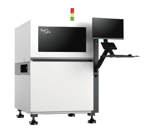
Applicable for AOI visual inspection in SIP packaging process stages, particularly effective for detecting surface foreign matter, scratches, lifted leads, and floating height on chips.
Deep learning AI algorithm
Deep learning algorithms enable neural networks to automatically learn features and extract information from massive data through training, performing intelligent analysis on image or video data. The current software integrates five universal algorithms based on CNN and Transformer architectures: classification, segmentation, object detection, character recognition, and unsupervised learning (good product learning). These algorithms demonstrate significant effectiveness in practical applications such as defect recognition in complex environments, component classification, and character reading scenarios. With deeper research, we have not only refined existing model architectures to reduce parameter quantities but also leveraged NVIDIA's efficient deep learning inference engines to implement computational graph optimization, accuracy improvement, layer simplification, multithreading, and batch inference processing. These enhancements have substantially improved model inference speed and efficiency.

· True 3D inspection for mirror-finish dies with positioning repeatability ±3μm and height repeatability ±1μm
· Detects components with pitch down to 50μm
· Delivers superior 3D inspection performance for high-reflectivity components and miniature components (008004inch)
· Proprietary AI technology enables detection of scratches, cracks, foreign matter at any die location
· Customizable vacuum adsorption fixtures supporting minimum product thickness: 0.1mm

· Camera configuration: 25MP industrial cameras ×3
· Lighting configuration: RGBW four-color LED multi-angle lighting system (standard coaxial lighting included)
· Resolution: 3.1μm
· Inspection speed: 5.1cm²/s
· Detectable defects: Chip contamination, edge chipping, corner missing, scratches, dents...
· Equipment uptime: 24 hours
