Home
About us
Products
SMT
Assembly test
ICT/FCT
Semiconductor
News
Partner
Contact us
Language
中文版
English
Submit
Products
Products center
Semiconductor
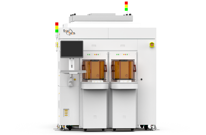
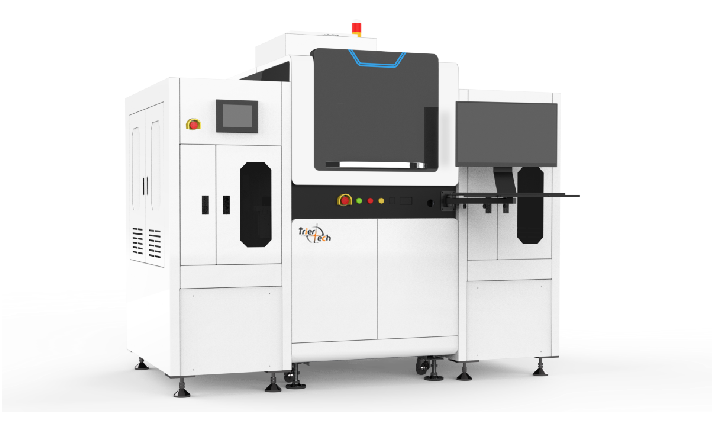
Wafer-level 2D+3D metrology inspection equipment
Applicable for die surface defect inspection, dicing street defect inspection, RDL defect inspection before/after wafer dicing in advanced semiconductor packaging, as well as bump height and coplanari...
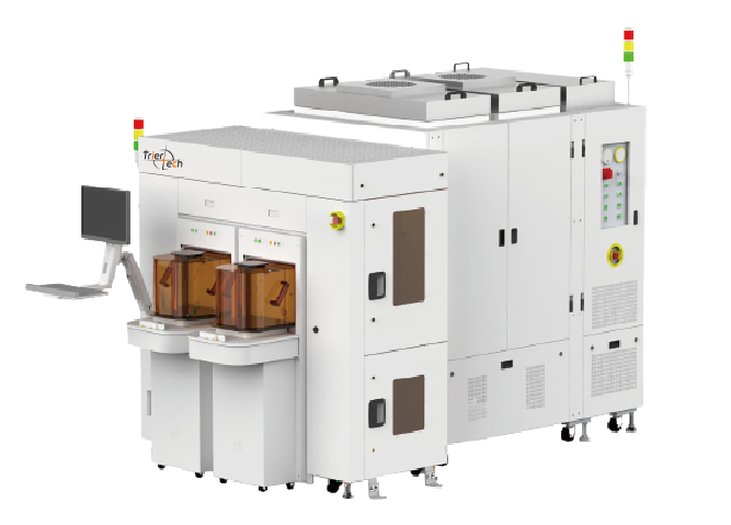
Post-dicing wafer defect
The equipment is applicable for post-dicing chip edge chipping, cracks, scratches, and surface contamination/residual glue detection in advanced semiconductor packaging.Deep learning AI algorithmDeep ...
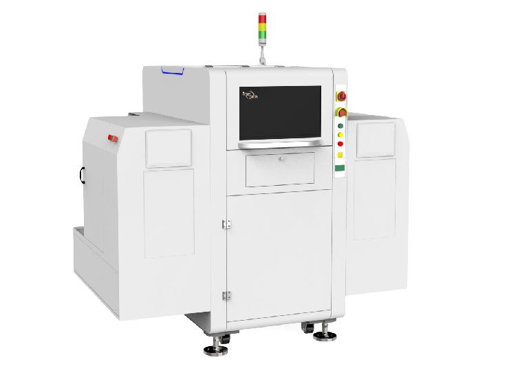
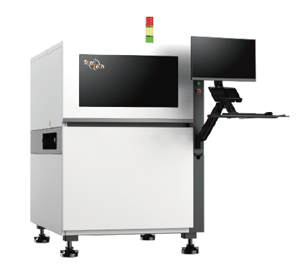
High-precision 2D+3D AOI
The equipment is applicable for post-packaging inspection of die surface defects after Die Bond and Wire Bond processes in semiconductor back-end assembly, as well as solder joint and gold wire defect...
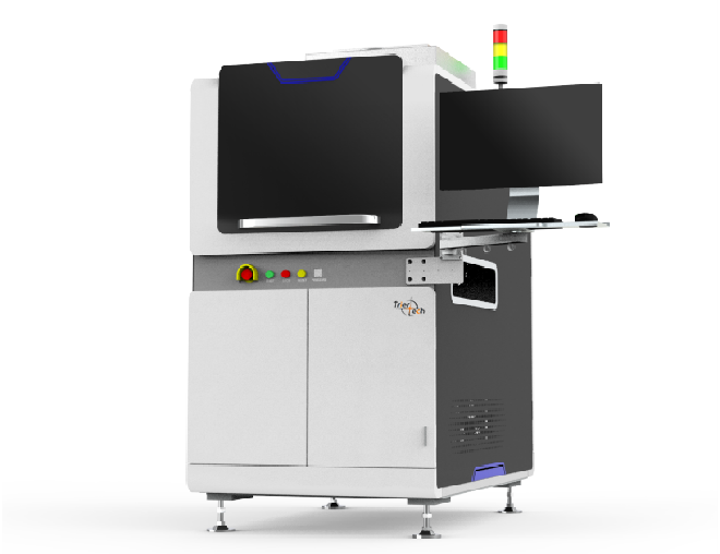
Micro-assembly specialized 3D inspection equipment
The equipment is applicable for micro-assembly Die Bond and Wire Bond post-process die surface defect inspection, as well as solder joint and gold wire defect detection after gold wire bonding.Deep le...
IGBT-specific 3D
The equipment is applicable for surface defect inspection of chips/DBC/trenches after Die Bond and Wire Bond processes in power semiconductor packaging and testing, as well as solder joint and aluminu...
Semiconductor SiP-specific AOI
Applicable for AOI visual inspection in SIP packaging process stages, particularly effective for detecting surface foreign matter, scratches, lifted leads, and floating height on chips.Deep learning A...
Phone
Home
Code